-
TSMC will start IC manufacturing at its A16 node (1.6 nm) in 2026
-
The clues we have indicate that it will not use high-aperture UVE equipment up to its 1 nm node
TSMC will start manufacturing 1.6nm ICs in 2026. This is not a guess; This was confirmed by CC Wei, the company’s CEO, just a few hours ago at the North America Technology Symposium event held in Santa Clara (California). This movement is much more than a declaration of intent; It is clearly a wake-up call to an Intel that is determined to take away from TSMC the leadership it currently holds in the semiconductor industry.
“Our technology will dramatically improve chip density and performance […] At TSMC we offer our customers the most complete suite of technologies so they can make their artificial intelligence (AI) projects a reality using the most advanced silicon technology in the world,” Wei said during the Californian event. This announcement aims to draw attention in a time when Intel and Samsung are fine-tuning their strategy to increase their market share to the detriment of TSMC’s as much as possible.
Intel’s ambition has forced TSMC to step on the accelerator
Intel’s short and medium-term plan to grow as a semiconductor manufacturer is shocking due to its great ambition. And, curiously, the extreme ultraviolet (EUV) and high aperture lithography equipment that the Dutch company ASML is already manufacturing plays a leading role in its strategy. In 2025 it will begin to carry out the first product tests using this machine, although the first integrated circuits produced with it will come out of node 14A during 2026.
In 2025, Intel will begin conducting the first product tests using high-aperture EUV lithography equipment.
Already in 2027 Intel will launch a presumably improved revision of this node that will be named 14A-E. These two nodes will mark the start of chip manufacturing using ASML’s new UVE and high aperture lithography equipment. According to Intel these machines will help IC manufacturers that they bet on them to sustain Moore’s law for longer. Both ASML and Intel argue that these machines have been designed to help semiconductor manufacturers increase the resolution of their lithographic processes without increasing complexity.
The path that TSMC is going to follow is different. Kevin Zhang, vice president of business development at this company, maintains that they do not need ASML’s high-aperture UVE lithography equipment to manufacture chips at their A16 (1.6 nm) node. It is evident that they are confident in their ability to optimize the processes involved in the production of integrated circuits on conventional EUV machines. In early January, Szeho Ng, an analyst at China Renaissance, predicted that TSMC would not use ASML’s high-aperture UVE equipment until it introduced its 1nm integration technology.
The DigiTimes Asia media, which usually handles very reliable information, has gotten wet and, like Szeho Ng, defends that TSMC will not use ASML’s most advanced lithography equipment in its 2, 1.6 and 1.4 nm nodes . If so, this decision would have very important repercussions. On the one hand, TSMC’s position reminds us that with appropriate refinements, first-generation UVE lithography equipment can be used to produce 2 nm chips, and even beyond (we will see with what performance per wafer).
And, furthermore, if TSMC finally confirms this strategy, it would not begin to mass produce integrated circuits using ASML’s UVE High-NA machine until the end of this decade. Probably until 2029 or 2030. We’ll see how Intel does with these devices. It is possible that if Pat Gelsinger’s bet goes well, this American company will be able to place cutting-edge chips on the market at a very competitive cost. This is precisely one of the assets that, according to ASML, its most advanced lithography equipment proposes.
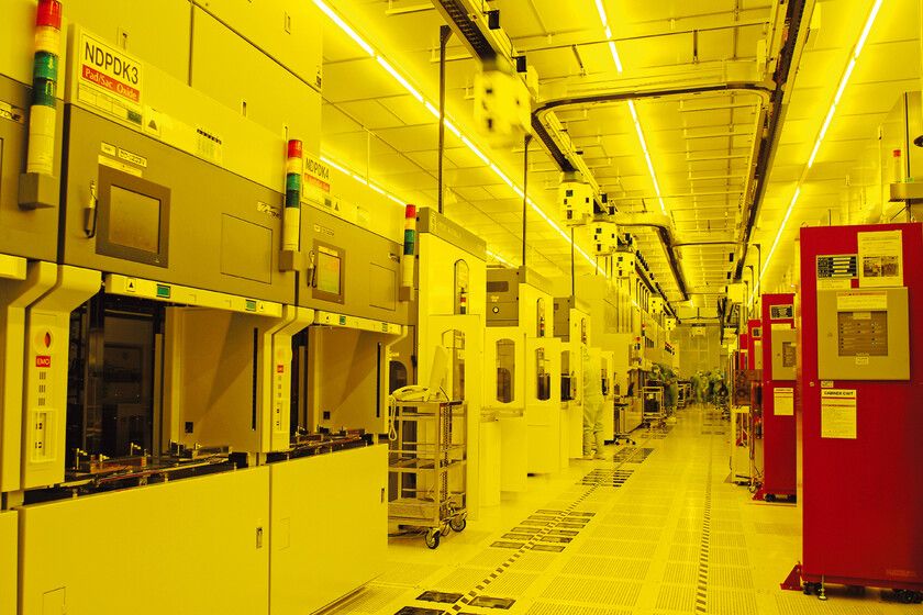
Image | TSMC
More information | Nikkei Asia | SCMP
In Xataka | Debacle at TSMC: American and Taiwanese workers clash at its new Arizona plant


